Electrical and Computer Engineering

610 readers
1 users here now

Electrical and computer engineering (ECE) community, for professionals and learners. Discuss ECE related topics here, for instance digital design, signal processing, circuit analysis, electromagnetics, microelectronics, power electronics, RF electronics, etc.

founded 1 year ago
MODERATORS
26


This Mastodon post hit #1 on Hacker News today, I think people around here would be interested.

Then you look at the $350 price point and walk away.

27


Atmel / Microchip created this Application note on how to drive the low-power and low-cost LCD segment displays.

However, LCDs should be energized with AC signals, due to their internal capacitor-like structure. No worries: microcontrollers can send AC signals thanks to PWM-like on-off sequences. But thinking about this AC signal and how it energizes LCD segments is rather complex if you've never done it before.

In fact, the electrical hookup here can be more complex than you expect. Its still a cheap hookup only requiring resistors directly connected to the pins, but... you need to think about this.

Note: If you're only doing a simple "Static" LCD, a simpler application note (https://ww1.microchip.com/downloads/en/Appnotes/doc2569.pdf) will be sufficient.

But some LCD screens, especially the ones with more segments, will have multiplexing. And multiplexing requires a more complex signal and electrical hookup to accomplish successfully.

28


Seems like a curiosity that people would like here.

29


Wurth is one of the biggest capacitor companies in the world, and they gave this webinar about 7 months ago.

I haven't watched it yet, but skipping through it looks pretty high quality. Alas, at 50-minutes, its a lot of information. So I'll have to watch this a bit later.

But for a lot of beginners and intermediates out there, yall might not realize just how complex capacitors actually are. There's the dielectric material (aka: chemistry), there's size, there's various ratings, and more. Its difficult to find comprehensive rundowns like this video. Beginners/intermediates should definitely seek out this kind of information, to make sure you're buying the correct capacitors for your particular tasks.

30


cross-posted from: https://lemmy.world/post/9234776

I think I've covered the material needed for a beginner to analyze and choose microcontrollers. However, a beginner may not be comfortable with reading datasheets, or families of datasheets. As such, I'll help beginners through microcontroller families.

This skill where you can download a few spec-sheets, analyze them, and understand them is an absolutely necessary skill. There's hundreds of chips released every year from many manufacturers. And while practice with a specific chip is the only way to true expertise, there's still the "breadth" of knowledge that comes in handy when selecting chips.

In this guide, I'm going to deep dive into AVR EA, the newest 8-bit AVR microcontroller from Microchip. But with commentary to help beginners understand the "big picture", how to evaluate this line and compare/contrast with other lines of chips.

Why so many chips?

Beginners might be flabbergasted to learn that there are 1498 available AVR-chips for sale, despite only ever being made by Atmel/Microchip. Of these, 1298 chips are the 8-bit AVR with mostly the same assembly language since the early 00s.

AVR itself refers to the instruction set (https://ww1.microchip.com/downloads/en/devicedoc/atmel-0856-avr-instruction-set-manual.pdf), the assembly language / machine code that makes up all of these chips. Development tools (compilers, linkers, IDEs) are built on top of this ISA and therefore cannot change very much in practice.

But many other features and specifications: the number of timers, 8-bit ADC vs 12-bit ADCs, DACs, UARTs, SPI, etc. etc. can and do shift on a regular basis. And ultimately, that's what leads to this chip proliferation. Its almost always possible to find a chip that does exactly what you want it to do, at the lowest price, at the lowest power-usage. So there's a lot of marketing and swapping of features to create a perfect chip for every application.

Microchip's AVR EA Family: (2nd) Newest 2023 era chip family

So lets get started at looking at the AVR EA. (Oh no, while I was writing the AVR EB was released and I'm too lazy to switch now... oh well...).

The webpage is a great starting point (https://www.microchip.com/en-us/products/microcontrollers-and-microprocessors/8-bit-mcus/avr-mcus/avr-ea ), but this only introduces the AVR EA family in general. We still have ... well...

All the other chips within the family. Now the main thing here is 28pin, 32-pin, and 48-pin pinouts... as well as 16kB, 32kB, and 64kB of Flash. Fortunately, the AVR Instruction set, and all the hardware (ex: Timer specifications, RTC, GPIO configurations, etc. etc.) are shared with recent chips (AVR EA shares very similar drivers with the AVR DD, AVR DA, and AVR DB chips released in the last 3 years).

The homepage contains the following line:

The AVR EA family of MCUs is a great option for closed-loop control system designs and secondary monitoring devices for safety reasons.

I agree with Microchip here, but how and why is this the case? What features from AVR EA make it ideal for this? Well, all in due time.

Curiosity Nano / Development Boards

All manufacturers create a "Development Environment" to help speed up experimentation with new chips. AVR EA is no exception, with the ~$25-ish AVR EA Curiosity Nano.

https://www.microchip.com/en-us/development-tool/ev66e56a

There is a USB programmer on board that works with MPLab and the legacy Atmel Studio IDEs, so you can easily develop from scratch (even without buying a special purpose programmer like Atmel ICE or building an AVRDude).

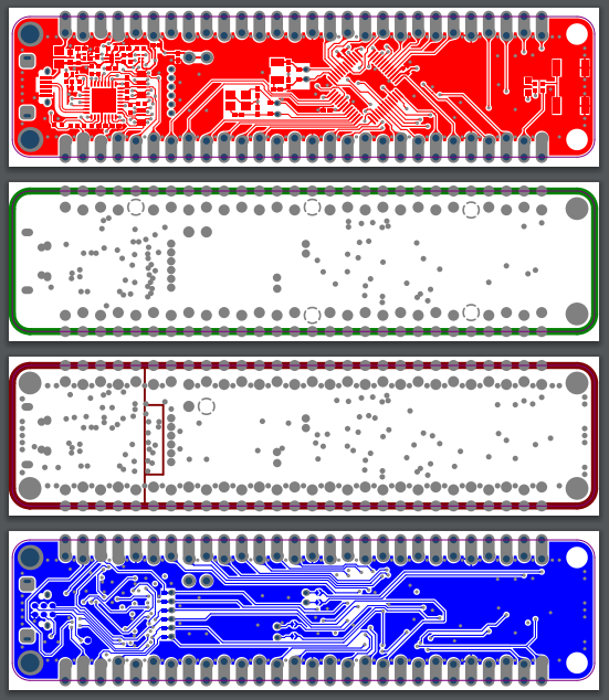
Microchip also releases schematics and PCB designs for these development boards. We can see that the AVR EA Curiosity Nano is a 4-layer board for example. All the relevant docs are in that area.

Chip Programmer

If you leave the prototyping stage and start making custom PCBs, you'll likely find a programmer useful for your later-stage prototypes on your custom boards.

https://www.microchip.com/en-us/development-tool/PG164100

MPLab Snap is the $35 lower-cost programmer from Microchip. I've never used this tool, I'm using a legacy "Atmel-ICE" (which used to be the $35 range, but it looks like MPLab Snap is replacing it). For Atmel-ICE, I've never had a problem just connecting over USB, running the wires to my board header and sending the code through. I'd expect MPLab Snap to be similarly easy.

Programming and Software

Atmel Studio (now Microchip Studio) is my preferred IDE, but it is considered legacy. Microchip Studio still is a free download and still work with AVR EA chips today (just tested with my Version4 of my Battery-tester project).

https://www.microchip.com/en-us/tools-resources/develop/microchip-studio

I've only ever used the free and open-source GCC compiler for AVR.

Microchip has been pushing hard for https://www.microchip.com/en-us/tools-resources/develop/mplab-x-ide , and I'd expect it to replace Microchip-Studio any day now. I do prefer the Visual-Studio based IDE though, but its hard to complain about free tools that work.

Microchip also sells their XC8 compiler, and there's other compilers like Keil or IAR. But professional compilers are $1000+, and likely outside the range of hobbyists / beginners who are just getting started. In either case, the $0 GCC compiler and toolchain exists and works with both the $0 Microchip Studio IDE and $0 MPLab X IDE. There is a free version of XC8 as well that is missing a few features, but should be usable-enough for beginners.

All of these tools provide the C-programming language (and maybe even C++ programming language), as well as linkers (combining .o object files together), the ability to create libraries, and a few libraries to help handle basic problems (Printf, atoi, etc. etc.).

Some people prefer Arduino software, I don't know much about it and have always preferred the low-level C stuff personally.

Can we talk about AVR EA yet?

Oh wow, yeah, I guess that's a lot of cruft beginners need to know before they get to the chip. Lets start talking about the chip now!

Digikey has thousands in stock across 66 SKUs. Larger quantities can be ordered directly from Microchip in 5000+ at-a-time quantities (though it can take some weeks for larger quantities to arrive). Both Digikey and Microchip offer the Curiosity Nano development board that I talked about earlier, and that might be a better place to get started than the raw chips.

But anyone thinking ahead to the custom-PCB phase of your project should see the SOIC, SSOP, TQFP, and VQFN packages of various sizes are all available. With some at extended temperature ranges as well.

https://www.microchip.com/en-us/product/avr64ea32

The AVR64EA32 in TQFP was what I used for a most recent project. The 64kB Flash and 32-pin layout shares much in common with AVR DA, DB, DD, and older chips (very similar layout, size, pinout, and pcb-footprint), so I prefer using that over-and-over again in different projects of mine.

HTML Version: https://onlinedocs.microchip.com/oxy/GUID-838DDB25-4D69-4519-815B-A48DBACEED23-en-US-9/index.html

PDF Version: https://ww1.microchip.com/downloads/aemDocuments/documents/MCU08/ProductDocuments/DataSheets/AVR64EA-28-32-48-DataSheet-DS40002443.pdf

Entering the manual, we have 565 pages of documentation. This is pretty small for modern chips, and this is due to the relative simplicity of 8-bit chips. (Many 32-bit chips are closer to 2000+ pages long). There's no need to read every single page of the manual, but instead immediately bring your focus to the following pages.

The first pages are a 5ish page summary of all features. I'm not going through the entire list, but I want to draw attention to:

12-Bit ADCs are available on a lot of chips these days. But Differential and PGA are eyebrow raising. These are relatively rare features that are incredibly useful in the application of current-sensing. This suggests to me that the AVR EA is for reading current and reacting to current-changes (such as the 4-20 mA current loop protocol). This is absolutely the "killer feature" of the chip, and is the reason to pick AVR EA if you have any current-sensing use in your application.

Most chips have a "killer feature" like this somewhere. It could be very high memory (264kB on the RP2040), it could be incredibly accurate ADCs (RX23E-A), or whatever. Knowing and remembering that this AVR EA chip is extremely useful for this niche is something you'll have to keep in mind for all future projects, thinking of what the best chip for your project could be.

Next, you'll want to look at the port multiplexing.

Only some features are available on some pins. AVR chips are more flexible than most thanks to the Event-system (some outputs can go onto the event system and be routed arbitrarily), but outputs are often tied to just a limited number of pins. If you're making a PCB layout, you'll have to keep these pin-multiplex issues in mind.

From there, skip all the features and just read the Electrical Characteristics. Keep in mind your voltage-levels, the capabilities of pins, and any features of the hardware you're interested in.

Don't forget Application Notes

Going back to the AVR EA landing webpage leads to the documents section. Check it out.

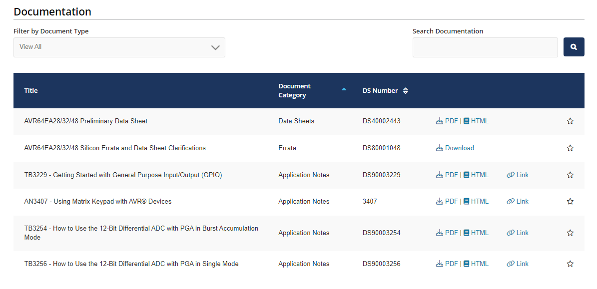
If you're not experienced enough to see the "killer feature" of a particular chip, look at the App Notes. They likely suggest situations that the chip is good at. They're trying to sell you this chip after all, but these App Notes (despite being marketing / sales purposes) are still good technical information that will teach beginners how to think about projects.

In particular, https://ww1.microchip.com/downloads/aemDocuments/documents/MCU08/ApplicationNotes/ApplicationNotes/AN4811-CurrMeasurem-BattMon-DS00004811.pdf

AN4811 is an AppNote covering how a 12-bit Differential ADC with 16x PGA (on the older ATtiny1627 chip, but still applicable to today's AVR EA) can be used as a battery monitoring / Coulomb counting application.

Honestly, I'd say that these Application Notes are the #1 source of information for beginners and intermediate engineers who need some hand-holding to learn how to use these chips (or chip features).

Thats it, I guess?

Well, I don't want to hold up everyone with an even longer article. But I think I've covered the crux of how to read a real world Microcontroller datasheet. There's hundreds of other pages in the datasheet and not enough time to cover it all, but I think I was able to at least cover the basics.

Would anyone be interested if I gave a rundown of my AVR EA Battery Tester project some time later?

31


I was reviewing a recent project of mine, comparing the LTSpice simulations vs my real physical circuit, when I noticed that there are effectively two independent ways of measuring "ESR".

So lets slow down for beginners for a moment. When EEs teach resistors, capacitors, and inductors to students, we are basically lying to you. There's no "ideal capacitor". All capacitors exhibit parasitic elements (aka: acts a little bit like a resistor or inductor), and not like the ideal math from the beginner world would imply.

But there's a 2nd layer to this, and it hits at the core of ESR/Impedance vs Dissipation Factor. Depending on how you test these parasitic elements, the value will change, sometimes dramatically.

Lets look at the 330uF WCAP-ASLI capacitor I chose for my project more closely. https://www.we-online.com/components/products/datasheet/865080145010.pdf

DF is created with one test, while the "Impedance" value here is a separate test. (Note, there is a frequency-dependent component with these parasitics, but according to RedExpert, frequency doesn't affect us in this particular discussion). https://redexpert.we-online.com/we-redexpert/en/#/redexpert-embedded

Also note: the ESR in this graph has been measured to be under 200mOhm (so yet a 3rd, completely different value to add to our mix!! Hurrah, I'm going to ignore this one, I've got enough trouble just talking about the other two "ESR" values already calculated in this topic...)

So DF is supposed to be related to ESR with the formula: ESR = DF / (2 * Pi * Frequency * Capacitance), or ~0.95 Ohms in this case. But... ESR/Impedance has been measured to be 0.34 Ohms, a rather substantial difference. What gives?

I'm going to admit that I'm now entering the realm of ignorance. I don't know why we have to different tests for what amounts to be an ESR test. But what I can say is that DF is measured at 120Hz, suggesting that the DF is more applicable to 60Hz power-line mains. While Impedance/ESR values are tested at higher-frequencies, suggesting a test more applicable to boost/buck converters or the like.

Since the values / specifications of ESR differ so grossly depending on "how you test for it", it behooves the EE to not only read these specifications, but understand the tests behind the specifications. So that we can better predict what will happen in reality. I assume that anyone building a full-bridge rectifier at 60Hz power lines (or 120Hz after rectification) will want to use dissipation factor values instead.

In particular: it seems like the Dissipation Factor (and the ESR-calculated-from-dissipation factor) is a strong estimate on the amount of Watts-of-heat generated from a 120Hz power-line (after full-bridge rectification). For some applications, its this heat generation that's the most important thing to calculate.

But for my purposes, where the capacitor is basically a decoupling / energy storage capacitor, Dissipation Factor (and its associated ESR of 0.97 Ohms) is not a good estimate on the final ripple going into/out of my boost converter. In this case, the Impedance value above (ie: 0.34 Ohms) is a superior estimate to what's happening in my circuit.

And this is engineering. Understanding not only the specified values, but choosing which value to think about deeper depending on context. The EE-world is full of little contradictions like this.

32


Lcamtuf conducts the classic "Hook up a signal generator to a coax-cable" to study some basic transmission line theory.

33


So I made an antenna based on a design on thingiverse/blog post. IIRC this is some Yagi variant. I did the math and did a bunch of tedious stuff to try and make it a proper project at the time. I do not have a network analyzer, smith charts are for shaman/wEEzards, and radio is the work of the devil. I was looking to extend the range of the 2.4G channel across my house just slightly using directionality. Empirically, it worked at first. I'm here half trying to diagnose, and half trying to understand some fundamental circuit design basics. The 2.4G output has two channels coming from the same peripheral radio chip. Normally these go to the dipole antennas. I used the same micro coax connector and proper coax throughout, with proper grounds/solder station/flux/etc. The continuity tests good still. The router automatically tries to move the transmit and receive signals between the two separate 2.4G channels under normal operation, but it drops one channel regularly now. I can see this on the network status of a connected device, and the drop happens regardless of proximity. I have not physically tested that the dropped channel is the one that had my DIY antenna. It could be a software problem. My curiosity is could this asymmetry cause a common failure mode, other than something obvious like ESD?

I etch, design, KiCAD, toner transfer, photolithography, and Arduino my way around in this space as a hobbyist, but like, I'm too lazy to go on the eevblog forum to ask this formally and radio is magic IMO.

This is the output stage in a bad hand held half ass pic with no attempt to do things like clean off the residue on the chips from the thermal pad that rests over them. terrible-image

34


Preamble: I have been pushing the "I believe" button for way to long when it comes to crystal oscillators and their supporting components. The concept is simple, as they generally consist of proper loading and some kind of (pre)amplifier. "Small thing shake fast and you amplify". However, the full concept has never "clicked" in my brain and it feels like a huge knowledge gap that I should have filled years ago.

Asking these questions is horrendously embarrassing since I am a licensed ham and I should intuitively understand how all resonant circuits work by this point in my life. (Hopefully, y'all have a better way for me to visualize resonant circuits in general.)


From this schematic, all I see is a DC source, an amplifier, and maybe a super-simple RC tank circuit (of sorts) and the wave should never drop below 0v:

Some of the most basic crystal schematics (concept diagrams?) show a crystal connected directly to an AC source.

The concept of a crystal is simple: Apply a voltage and it moves, remove that voltage and it returns to its original shape. That kind of explains why kick-starting oscillation is needed, but that is not really where I am confused.

My questions are:

Is the crystal more closely related to an inductor in a basic RLC circuit? Is L being an approximate relationship to X a good way to visualize this?

Does the crystal "force" an RC resonant circuit to operate at a specific frequency because of its tendency to only operate efficiently at a given frequency in wildly different environments? (This question is a result of the first: Does an inductor act like a crystal in some ways?)

Since basic BJT amplifiers are generally shown with super-basic crystal schematics, is that amplification a functional part of generating a wave form? So, if the BJT was removed, the circuit would still function but it would be at a much lower current? (TBH, I am getting a gut feeling that the BJT is functionally related to an opamp with feedback in the above schematic, maybe?)

Thanks in advance for any education. Cheers!

(Oh, I do understand we are mixing AC and DC circuit concepts here, so that isn't an issue for me either. I also could just "look at the formulas" for building crystal circuits, but I need a better understanding of the core concepts first.)

35


So I was thinking about Flash memory today, and I realized that the FTL / Flash Filesystems are overly-complicated for a lot of microcontroller applications. Still, microcontroller projects need some way to ensure that the NAND Flash wears out evenly (some uCs, like the AVR DD, only has 10,000 erase/write cycles on its Flash).


The traditional answer is of course, FTL (Flash Translation Layers), a component of modern Flash-based filesystems. As a modern filesystem writes data, the FTL remembers how many times each Flash-page has been written to. The FTL / Page allocation logic ensures that the least-used page gets malloc()'d next, and therefore balances the erase cycles across all the flash to maximize endurance.

In particular, when the application code wishes to "erase" a Flash page, it instead is "malloc()" from the pool of flash (usually: the one with the fewest erase cycles), while the old page is conceptually free()'d back into the pool. (a process known as "TRIM" on modern Flash controllers)

This way, as the application-code writes files (or rewrites files), the FTL walks across the whole flash and load-balances the erase cycles.

Things can get far more complex (ex: static wear leveling), but this is enough of a discussion that I think beginners can follow along now.


Anyway, the FTL itself needs a wear-balanced data-structure. I can imagine a few off the top of my head (writing to a journal-like log of FTL pairing changes)... where the Microcontroller would read the whole log upon startup and "recreate" the most recent data (ensuring integrity even in a random power loss). After all, the FTL itself needs to be persistently stored, and the best place for that is... well... the Flash system you've got. So FTL persistent storage data-structures necessarily solve this problem.

But I was wondering: is there a book, an encyclopedia, or other such reference which discusses wear-leveled data-structures such as the FTL?

I have to imagine I'm not the first programmer to think about using these 64kB or 32kB Flash Microcontrollers in a wear-leveled manner. Someone out there must have implemented something and wrote about it!

EDIT: For my research, I'm looking into JFFS2, YAFFS, and other Flash-based embedded filesystems to see if their source code has any references to anything, or other such concepts. But if anyone has pointers for me on this question I'd be very interested!

36
37


To get myself back into electronics, I pulled out an old project idea I've been wanting to do for a while, and that's a AA NiMH battery tester. I have a collection of ~30+ AA NiMHs that I use for various purposes: Flashlights, Switch Controller (yeah, they made an attachment), Electric Toothbrush, Walkie Talkies, etc. etc.

After a few years of abuse, these AA NiMHs degenerate, but at different rates! Even though I bought them all at roughly the same time, different levels of abuse made some cells barely hold a charge, while others work almost like new. How do I differentiate between them?

Simple: charge up the AA cells, then perform a current sensor / coulomb count against them. That is: measure the current out x time taken == total amp-hours that a particular AA cell can take. And if this value drifts too far away, I recognize it as a busted cell and send it to my local Home Depot for recycling.

First, I'll go over the schematic one-at-a-time for everyone.

V3? What's version1 or version 2?

Erm.... mistakes were made. Lets not talk about V1 or V2 right now...

7 Segment LED Driver

The "Digital" half is pretty simple, I take the surface-mount ACDA02-41SURKWA-F01 (https://www.digikey.com/en/products/detail/kingbright/ACDA02-41SURKWA-F01/3084667) 2-character 7-segment LED x2, and hook them up as appropriate to an AVR DD microcontroller.

At 3.3V Vcc and 1.6V Vforward LEDs, a 820 Ohm resistor will let ~1.8 mA of current, which testing has shown to be plenty bright enough for my purposes.

For the newer EEs out there, these devices are very dumb.

https://www.kingbrightusa.com/images/catalog/SPEC/ACDA02-41SURKWA-F01.pdf

These "Common Anode" LEDs have high-voltage all running from the same wire. So they only work with a little bit of microcontroller magic: I turn on one-digit at a time (ex: Digit#1 goes to high-voltage, then I can display a 0 with the binary output "11000000" (low-voltage on segment abcdef, and high-voltage on segment g).

I then turn Digit#1 off (set voltage to low), and then set Digit#2 to high, and display the same ports "10011111", which will display the "1" character.

Etc. etc. I can cycle through Digit1, 2, 3 and 4 a thousand-times per second so that the human eye cannot see them changing so quickly. This ultimately displays a 4-digit number.

Battery, Current Sense, and Instrumentation Amplifier

The battery is just that: a single AA-battery holder. The entirety of this circuit runs through the 0.1 Ohm current sense resistor, meaning even the power behind the microcontroller/LEDs gets "counted".

For beginners out there: an OpAmp is an "analog computer", allowing electrical engineers to add, subtract, multiply, divide, differentiate, or integrate voltages.

An Instrumentation OpAmp is a specialized OpAmp that focuses upon differential signals and multiplication with a constant (aka: C * (A - B) type calculations, where C is a constant). In particular, Instrumentation Amplifiers increase the accuracy of the (A - B) calculation by maximizing the CMRR (common mode rejection ratio), aka the "minimization of error from changing voltages", and PSRR (Power Supply rejection ratio), aka the "minimization of error from changing power-supply".

As a tradeoff, Instrumentation OpAmps have worse bandwidth and less flexibility.

A Zero-Drift Amplifer is a further specialization that focuses upon very low offset voltages (aka: the where the OpAmp thinks 0-voltage is located in reality).

Nominally, you could use a general-purpose OpAmp, but its always best to pick the specialized amplifier for any particular job. As such: I picked the MCP6N16-10 is a Zero Drift AND Instrumentation amplifier. Because its zero-drift, it has 20uV specified offset voltage (or 0V will be somewhere around +/- 0.00002V in reality). There's a further requirement that the MCP6N16-10 only works if I set the gain (aka: the "C" in C * (A-B) calculation) at 10x or higher.

In this case, I set the gain at 27.3.

Now lets step through what happens here: When say 500mAmps rushes through the current-sense resistor

V = I * R

Thus, the 500mA * 0.1 == 0.05V change across R1. MCP6N16-10 very accurately performs (R1_high - R1_low) calculation (thanks to very low offset voltage), and thanks to the 27.3x multiplier, will output 1.365V.

I then added a 100k / 10uF simple low-pass filter for anti-aliasing as well as averaging out in the analog domain. This effectively creates a moving average of the most recent ~6.28 seconds. (Or perhaps, I have a low pass filter with Fc of 0.16Hz if you want to think about it in the frequency domain).

After all that, it goes into my Microcontroller. I've configured the AVR DD to have a 2.048Vref for the ADC. Alternatively, you can think of the 27.3x multiplier + 0.1 Ohm resistor + 2.048V Vref and 12-bit ADC to reasonably accurately measure resolutions of ~180 microamps per least-significant bit, across ~0mA through 750mA or so worth of nominal range.

All resistors are +/- 1%, though the Vref of the microcontroller is +/-4%.

The load

A very simple low-side NMOS switch driven by the AVR DD. More on this later, I think I made an error with this version that I'm fixing in my next design. But the uC simply drives the NMOS high to let the 2.2Ohm resistor send ~500+ mA across the battery.

The 3.3V Boost Converter

Various parts on this board require more voltage. The whole board is powered by only a single AA cell, which will vary between 0.9V to 1.4V depending on how charged the AA cell is.

The boost converter takes this voltage / current / power, and converts it into 3.3V. The design here is simply following the MCP1640BCH data-sheet, and then picking new resistors that were found elsewhere on my board (instead of the original resistors that were in the docs).

KiCAD Notes

KiCAD is a free CAD tool to help create PCBs.

  1. Create and/or Select Symbols -- These represent the various chips and parts you'll put into your design.

  2. Create a Schematic -- KiCAD will use the schematic to automatically check which parts need to be connected to each other.

  3. Create and/or Select Footprints -- Each symbol is then given a footprint, the 2D representation of how it will look like on a PCB.

  4. Layout PCB -- First configure the PCB to have the settings of your manufacturer. click "Update from Schematic" to import data from step #2 and #3, and then just arrange the items in the PCB editor till things look good.

The PCB Manufacturer

I wanted to try out DKRed this time. https://www.digikey.com/en/resources/dkred

I chose the 2-layer PCB settings and configured KiCAD with the board specifications.

The PCB Design

It is impossible to have a solid ground-plane on a 2-layer board, but I made the ground plane as solid as I possibly could.

Of note is the PCB-heatsink on the right side of the board, as well as the "sideways resistor". Let me bring attention to the 2.2 Ohm resistor really quick.

https://www.digikey.com/en/products/detail/vishay-dale/RCL12182R20JNEK/2556524

This resistor is designed with "sideways" leads so that the heat would more easily transfer into a "PCB Heatsink". All a PCB Heatsink is is a large section of copper you leave for non-electrical reasons... but just for the heat-sinking reasons alone.

The Mistake: Bad EMI???

Did you catch the mistake? In my haste to maximize the PCB Heatsink size, I've removed the ground-plane from under the 2.2 Ohm resistor.

Now... maybe in isolation that's not a big deal. Except upon finding and testing this design, I've found that the rise-time of that NMOS is 20 nanoseconds in practice.

And when the voltage reaches near the 0.95V cutoff mark, the code will purposefully PWM to try to train the last bits of the AA cell down to the 0.95V cutoff. (When a cell is 0.94V, it cuts off the NMOS, but this immediately causes the voltage to increase back to about 1.02V, causing the code to turn the NMOS back on... causing the voltage to drop to 0.94V, etc. etc. at a rapid rate).

I'm fairly certain that I've got bad EMI noise in the 50MHz+ range in practice, though I don't really have a means to test it. My next version will be a 4-layer board with better respect for grounding issues.

As it turns out, a significant amount of the traces going to the 7-seg LEDs use a good amount of room (and also cut up the ground plane on the 2nd layer). So I think a 4-layer board will shave off a few more millimeters off the width of this design.

My next version includes a "slow start" capacitor on the NMOS, to have microseconds of risetime on the NMOS rather than the 20ns of risetime in this prototype. Also, with a 4 layer board, I should (theoretically) minimize any EMI issue that would come about (not that I really have a good measurement tool for that).

Prototyping and Assembly

I applied low-melt lead-free solder paste, manually placed all the parts with a tweezer. For those who have never used solder-paste, its pretty easy. Solder paste is sticky enough that the parts remain in the proper place after you stick them on. I did buy a solder paste stencil (~$10 these days) to make the application of solder paste braindead easy on my 3x prototypes.

I used the "Electric Skillet" method (turn on the skillet until the solder paste melts, turn off the skillet, then use hot-air rework station to fix any tombstones). Thanks to the magic of solder and surface tension, the solder itself will mostly pull themselves into the correct spots when the solder is molten. So you don't need to be very precise with your placement.

I used a x10 Loupe to inspect for solder bridges. Solder bridges were fixed with a soldering iron + solder wick. Once the surface-mount parts were all confirmed to be good, I added the AA-holder to the back and used traditional leaded-solder to attach the pin through the though-hole... erm... holes.

I'm fairly certain that I messed up the fragile oscillators due to neglect. My clocks are severely off, by 5% or so (the clock is supposed to be 20ppm, or 0.002% accurate, so 5% is severely off). So next time, I'll be more careful about my soldering procedure.

Programming

Microchip Studio is pretty straightforward, and I don't think the code is very difficult. I manually initialized the various hardware bits of the AVR DD by reading the manual.

Initialization routines have a recipe from the manual to follow and the documentation is rather straightforward. I did come across a bug with "AC_MUXNEG_DACREF_gc" being the wrong value (shame Microchip!! You messed up your .h files!!), but it wasn't too difficult to see the error when the code ran and I fixed it up in a few minutes. (manually used the value from the manual: 4).

Code is written in polling style, there's no OS here so I just have an infinite loop that's checking for the clock to change and reacting to the clock.

4096x per second, I update which digit I'm displaying.

1024x per second, I cycle through all 4 digits. I use 16-bit BCD so that I only need to bitshift + AND to extract the values in this most common operation.

64x per second I check the Analog Comparator for if the battery has dropped below 0.95V. If so, I turn off PortF (the NMOS).

16x per second I update the milliamp BCD number to display later. I have a very expensive division / modulus operation here, but the AVR DD even at 4MHz is fast enough to perform this operation without causing issues in practice. I also have a moving-average queue to average out the last 16 values (ie: 1 second), to help cut down on noise in the display.

2x per second I update the AmpHr number. AmpHr is a 64-bit fixed-point (32-bit above 1.0, and 32-bits for the fractional half).

1x per second I swap between AmpHr display and miliamp display.

The ADC updates as quickly as possible asynchronously. There are no interrupts, I simply read from the ADC regularly and add the ADC value to the 1/64th miliamp variables (which will be divided out / normalized later).

The code is only 250 lines long with substantial amounts of comments. I don't use interrupts, I simply poll with if() statements on all the above conditions. Everything completes fast enough ("realtime enough") that all the code just works without any of the complex features available to me.

Calibration

I pulled out my benchtop Fluke 45 to calibrate the ADC errors with a #define. This is an old benchtop multimeter with ~5 digits of display, giving me accuracy to 0.0001Amps of measurement. (Alas: the more accurate measurement of 100.00 mAmps only works at 100mA and less, and my design is 500mA).

I've noticed a decent amount of non-linearity. I wonder if I'm leaking current somewhere? Or maybe there's more offset error due to something unknown? Still, the overall error is within 1% across the range, and maybe I could calibrate both a zero and the 500mA points to help minimize this non-linearity.

Calibration is just me changing a #define in the C code. Nominally I have a 2k trimmer pot here, but it seems like #defines to trim away the error was sufficient in practice. Next version won't have the trimmer pot.

Questions?

Lemme know if anything doesn't make sense to yall. I don't think this is an especially difficult project. I hope I gave enough details so that the newer EEs in this community could follow along.

Feel free to ping me for questions. I know someone out there was looking for a current-sensor project. This is my current sensor project, probably different than what you are going to build, but maybe its a source of inspiration for you.

38


Anyone have a recommendation for a benchtop current sense amplifier?

Sure, there are current sense breakout boards and whatnot. But what I'd like is a convenient device that I can use to instrument a circuit and then monitor its current with my oscilloscope or logic analyzer (Saleae with analog input) along with other signals in the circuit.

Ideal features might be:

  • Banana jack inputs and outputs
  • Selectable range / sensitivity / sense resistor
  • Isolated measurement, so I can measure high-side or low-side currents without worrying too much about the common connection on my scope
  • Selectable or automatic power source selection, between circuit-powered and externally-powered

I haven't seen anything like this in a few targeted searches, and just wondering if someone has any suggestions I might have missed.

39
1
submitted 9 months ago* (last edited 9 months ago) by dragontamer@lemmy.world to c/ece@lemmy.world


Hey everyone.

I've asked the Lemmy.world admins to make me a moderator of the /c/ece community. I'm a ECE major from college, but all of my real-world work job is programming. So the only electrical/hardware stuff that I do is for hobby work. Still, I'd like to think I know a thing or two worth sharing.

I've got an imagined list of topics that I'd like to cover to help seed and generate discussion. But what would be helpful for me is to know the skill level of my audience. I'm sure there's plenty of experts who are stronger than me in the field of ECE, but I remember being a young high-schooler trolling around EE USENET asking stupid questions. So I also imagine a few precocious high schoolers out there might be lurking around.

So... what is your skill level? Who should I be writing for? Are you hobbyists with no formal training? High-school level with just a propensity to look at various Youtube videos? Or are you formally trained but no practical knowledge? What subjects do you think would be best that I covered?

Over at another lemmy, I've mused upon the skill levels I imagine: https://lemux.minnix.dev/post/81220

The skill tiers I think of are as follows:

Tier 0: Wires and "Lego" sets. Arduino-boards connected with Qwiic and/or Mikrobus

Tier 1: Breadboarding and Through-hole rapid prototyping.

Tier 2: Low speed simple PCB design. Large surface-mount parts.

Tier 3: Higher speed PCB design. Smaller parts to minimize parasitics.

Tier 4: Design with BGAs. "Transmission Line Theory" all across the board, delay matched lines

40


I'm working on implementing the PID compensator on the top of page 20 here. I've already got a circuit working, but it oscillates a ton, and I was hoping to tune it with a better strategy than just guess and check.

The datasheet doesn't go into a lot of detail on how it's supposed to work, but I found a whitepaper that covers single-stage PID compensators in more detail here.

I've got this compensator working, I've modeled it in spice and the poles and zeroes show up where they should, but I have no idea how to actually tune it to my system.

My understanding is that I need to fit the equation (3) on the second link to the form kp + kds + ki/s, but it's an algebraic nightmare.

What I'm hoping for is some derivation of the PID constants in terms of the components in my system. Then I can work on one of the many tuning methods. The datasheet even assigns names to components implying that they're responsible for setting one of the constants (Cd and Rd for derivative term for example), but I'm fairly certain they can't be completely isolated like that.

Also, if the answer is just that I need to re-learn how to do partial fractions, I'm okay with that.

41


OSHPark's 6 layer service here: https://docs.oshpark.com/services/six-layer/

OSHPark has a 5mil trace/ 5mil-space specification, with 4-mil annular ring and 8-mil minimum drill size (ie: 16-mil minimum via sizes). For $15/sq-inch PCB boards with no setup fees or other costs, this is easily the best US hobbyist option for BGA service.

A 16-mil via is 0.4064mm. For a 0.8mm pitch BGA, that leaves .3936mm left over on the lower layers. 5-mil space (left-side) + 5-mil trace + 5-mil space (right-side) takes up .3810mm. On the top layer, BGA contact pads vary but 0.4mm contact pads seem common.

So that's a smooth 0.012mm left over (12 microns) for 0.80mm pitch devices. Not much room for anything smaller pitch. Still, it goes to show that all 0.8mm pitch BGAs (and larger pitched devices) are now easily available to hobbyists.

42


I am working on some extremely small designs where the entire board is less than 15mm2. There are a surprising amount of very small ICs but I've found it's really tricky to actually do a thorough part search for tiny (sub 2mm x 2mm) parts.

Some vendors have CSP packages that are relatively huge while having other package types like X2SON which are actually smaller. What was called 'tiny' and 'smallest' a few years ago is actually pretty large by today's parts.

Any tips on how to find parts?

43
1
submitted 10 months ago* (last edited 10 months ago) by dragontamer@lemmy.world to c/ece@lemmy.world


I noticed a few $20 screen+resistive touch screen (4-wire) being sold on Digikey, so I started looking into the 4-wire Resistive touchscreen info.

This app-note from Atmel (now Microchip) is a good introduction to this resistive screen style.

44
1
submitted 10 months ago* (last edited 10 months ago) by dragontamer@lemmy.world to c/ece@lemmy.world


While we live in a day-and-age of overwhelming microcontrollers, the Analog Sensor world continues. A few resistors, capacitors, and an amplifier (General Purpose, Zero-Drift, Instrumentation...) can likely still have far superior performance than $1, $2, or $3 microcontrollers in practice. Bandwidth, detection and analysis of microvolt-level signals, and all at lower costs.

Having a quickie "guidebook" for common configurations, indexed by application / sensor type is useful. Microchip made this .pdf and I personally found it very interesting. Hope everyone else likes it!

EDIT: Note that many of these circuits are available from an analog-chip. Ex: the current-sensor chips can be bought from Ti, Diodes, and other companies that have well-matched (and on-board) trimmed resistors, that basically implement the current-sensor circuit found in this document. So it still helps to know what's out there and study the part-libraries from various companies.


That being said: remember that in the year 2023, 18-bit sigma-delta I2C ADC exist with programmable-gain stages (~7uV of resolution raw, maybe even more resolution with higher gains). So always compare/contrast against a digital solution which might be easier to code/build than trying to deal with noise / other analog issues... especially if you're willing to sacrifice bandwidth and/or costs.

45


cross-posted from: https://lemmy.world/post/6104468

On the other community, I have a post (https://lemmy.world/post/5214451) where I rough out 5 tiers of skill.

  • Tier 0: Wires and Connectors

  • Tier 1: Breadboarding

  • Tier 2: Simple low-speed PCB Design

  • Tier 3: Beyond 20MHz PCB Design and Leadless chips

  • Tier 4: Transmission Lines and BGAs

This PCB Design Tutorial from Phil's Lab covers the big step between Tier1 and Tier2, perhaps the most intimidating step for most EEs. You're spending real money every "attempt" after all, as there are very few repair mechanisms you can make to a finished PCB. (though with enough skill with Xacto-knives and some "deadbug" style soldering, you can probably repair more PCBs than you thought was possible).

Phil is obviously talking about this design/layout problem from a "Tier3" perspective though, thinking carefully about the (unused) analog-lines with a Pi-Filter (capacitor - ferrite bead - capacitor), and trying to use high-speed layout techniques wherever possible. But the fundamental problem is actually Tier2 or beginner level, despite all the caution that Phil does here.

So this is a great video, not only for tackling a beginner friendly problem, but also for doing it from an "expert's eye / mindset". A beginner probably can solve this problem without as much thought/effort as Phil put here, but its good to build habits and your higher-tier skill levels even on this simpler problem.

Below is my original post from MICROCONTROLLERS@lemux.minnix.dev:

While this 1-hour / 40 minute talk may seem intimidating at first, its a complete beginning-to-end of building a custom STM32F1 PCB. This is probably best for someone trying to make the leap into PCB-design.

The STM32F1 is overall a beginner friendly chip, relatively low power and robust with a large community of people to ask for help on. I've never personally used this chip, but its got a solid reputation as beginner friendly.

Decoupling and Crystal-Oscillators are the hardest part of this particular schematic / pcb design. Electricity moves slower than a beginner expects: when a fast circuit (such as a 16MHz Microcontroller) takes in power, there is a "local power outage" as electrons "near" the chip gets sucked out, lowering voltage and potentially blacking out the chip, before the electricity begins to flow.

A decoupling capacitor provides a source of electrons during this brief, nanosecond-level blackout, improving reliability in your design. Its good practice to just scatter 100nF capacitors around Vcc/Gnd pins "just in case" (why bother running analysis when capacitors are a penny each?). This overall analysis is called PDN (power distribution network), but at Tier2 / just graduating off of breadboards level, let's keep the analysis simple and crude. You can make a masters degree out of this subject alone after all.

At Tier2 / low speed designs, it's as simple as throwing 100nF capacitors at each Vcc pin. This video makes things a bit more complex with a Ferrite Bead + 1uF Pi-network but beginners can completely ignore this aspect of the video (or even remove it from their circuit) and everything will still work (albeit the ADC will have slightly higher noise levels, but work nonetheless). I'd rather this advice that Phil gives at roughly Tier3 skill level. (Which is good for those who want to be a stronger PCB designer, but the absolute beginner can ignore this aspect).

Now Crystal-Oscillators are famously tricky to start and debug. Without measuring, your "16MHz clock" might be closer to 15.999927 MHz instead (~83ppm or worse) off. I think beginners "don't care" about this, but EEs are very peculiar about getting clock timing correct... aiming for +/- 20ppm at all temperatures and voltage conditions. If a crystal problem happens, I don't think the beginner has any ability to debug it (it requires a very low capacitance oscilloscope and other fancy equipment to properly debug a misbehaving XTAL), but modern chips are pretty robust in general.

Despite the potential hassles and roadblocks... I think beginners should try laying out the Crystal-Oscillator. If there's a problem, you can configure the STM32F1 to use its internal clock (which is only 1% accurate, or could be as far off as 15.8 MHz). So its a win if you lay it out successfully, and maybe just a minor-inconvenience if you fail at it. A good potential learning experience in any case.

The key here is that the beginner needs to be aware of potential clock problems and have a plan to test if something goes wrong. IMO, Phil here is aiming this video at maybe Tier3 or higher skill levels and assumes that the watcher can instantly make a plan (like I did in the previous paragraph), so it went unsaid in the video.

Things will go wrong in electronics. But we engineers figure out contingencies and learn to plan by doing things. Not much we can do aside from experience the failures (or successes) on our own to gain experience.

46


cross-posted from: https://lemmy.world/post/5751732

I posted this to someone else's Microcontroller Lemmy, but I want to see how many people at Lemmy.world might be interested in this kind of material too

In my most recent "Beginner Series" post, I classified skills from Tier0 through Tier4. This Tier4-level talk is about how to think of PCB-layout at the most complex levels, thinking about the precise forms of electricity and why-and-how it creates EMI fields, almost like an antenna at times. (Or perhaps: more like a capacitor when these waves travel across a PCB).

This video covers proper "grounding", or perhaps more accurately, proper "reference planes" where the electrical field between signal-and-return current can be defined. Thinking in terms of both signal-current and return-current minimizes the EMI (aka: antenna-like radiation) from coming off your PCBs. This is more of a problem of high-speed circuits and therefore I rate it as "Tier 4".

47


Hi,

I have a 20Ah 48v EV Lipo battery that I would like to use as a Powerstation. It uses a 2 pin + 4 data connector as seen in the link. Is that possible? What other hardware would be needed? Discharge controller/Voltage converter?

48
1
submitted 1 year ago* (last edited 1 year ago) by RickyWars@lemmy.ca to c/ece@lemmy.world


Hi all,

Anybody do RF/Communications Engineering in Canada? Tell me a bit about your experience. I'm starting my PhD in the fall.

49


I've been a systems engineer for about 5 years, and while I do appreciate the exposure to a bit more hardware than a pure software engineer role would give me, I still feel like 95% of my job is coding.

I've been considering switching to a DevOps role, and getting more involved with infrastructure.

My only real concern is that if I do this, it may be harder to break back into the engineering side if I ever decide I want to come back.

Does anyone have any experience or advice in this regard? Also, sorry if this isn't the best place to post this; Still trying to find all the new communities here.

50


cross-posted from: https://lemmy.ca/post/915272

QSPICE is a new and fast SPICE simulator written by Mike Engelhardt (author of LTspice). QSPICE was initially limited to beta testing in May, then expecting to become open beta testing in July.

Quick start gives a quick overview of the UI and other elements of the software. Below are few more videos on the features.

Importing 3rd Party Models: https://vimeo.com/828090312/aa254d2e95

Using C++ and Verilog in QSPICE: https://vimeo.com/828086789/a7ada3a5d3

view more: ‹ prev next ›