1
36
submitted 1 week ago* (last edited 1 week ago) by jet@hackertalks.com to c/electronics@discuss.tchncs.de

Built out my ploopy mouse today, it's been sitting on my shelf for a while. I got the self-assembly kit, had to solder on one through hole component.

So far I'm enjoying the mouse, the right mouse button is a little sticky, but I'm sure with a little readjustment it'll fall into place.

Every part of this mouse is open source, the hardware files, the PCB, the schematic, the firmware which is QMK. There's a lot to love here.

I've been playing some video games, and so far I enjoy the mouse quite a bit.

If I do have one complaint it would be the central scroll wheel doesn't have a detent, but that might just take some getting used to

I would love to see a kinesis style pinch mouse like the DXT2.

@pronk@mastodon.social @PKL@mastodon.social Great device, thank you for making it open source.

Note: I ordered their USB cables, just for solidarity, and assuming they found a cable that was very effective for a mouse, the cables I received were very strong, too stiff really to be used for a mouse cable. Luckily I had some very flexible braided USB cables already. So if you're going to order from them do not order the USB cable

2
32
submitted 2 weeks ago* (last edited 2 weeks ago) by jet@hackertalks.com to c/electronics@discuss.tchncs.de

A banger video about applying sintered traces to 3d printed models... BUT more interesting then that is the use of ChatGPT to "exfiltrate" unpublished formulas for the cooper plating solution.

In the video at 8:10 Ben goes through his exhaustive search of trying to make a solution that would work, and details that all the labs keep it more or less a secret, but the application of a LLM revealed the difficult to find steps/formula needed.

Obviously ChatGPT gobbled this up somewhere... just published on the internet but Ben didn't find it? Or did ChatGPT get trained on internal/corporate documents and the LLM is actually democratizing this information?

3
1

I got a Sylvania-branded strand of 50 "warm-white" LEDs (plus two loose spares) for USD 2.50 at the local grocery store, which I'm pretty sure is cheaper than buying a bag of the bare LEDs would run. They also come in other colours (blue, cool-white, bright red, multicolour)

The individual LEDs come in plastic shells which can be cracked open to retrieve the goodies inside, and have plenty long leads that are folded over to fit the "bulb" mounting.

4
1

This decade old electric cooler box gave up the ghost around 2 years ago, with the indoor outlet plug no longer working. The independent 12v input was still operational, so I kept it with the intention of eventually fixing it...

And two years later, this is the eventually 😅. The integrated 10v ~45w unit had failed short on the primary side, with a burnt out Y-capacitor and some fried zeners. I started removing bits from the board to try and find all the broken components... but ended up letting out the magic smoke in the process, oops!

I set out looking for a new power supply, and came across a 12v 45w unit from Meanwell. It was actually smaller than the cooler's original power supply too, meaning more internal space to use later 🤫

Spoiler

After searching for a distributor that was actually willing to ship it to a home address, I ordered, and boom:

It's so tiny compared to the original.

Next I installed an Arduino Nano to control the TEC/peltier module & fan via a cheap LED repeater. I was hoping to reuse the internal temperature sensors, but left them disconnected for now

After hours writing the arduino code, I finally got it into a usable state. There were issues with brownouts rebooting the Arduino, however with the Meanwell supply in-circuit those mysteriously stopped.

There are 3 power modes now for the module: 30W, 40W and 50W - with the first two using PWM, and the last one giving it all the beans. I wanted to PWM control the fan too, but decided against it since it sounded absolutely terrible at whatever PWM frequency the Nano is using.

It powers on to 40W by default, which is under the 45W max rating of the PSU.

Everything looks good so far running from the bench supply:

Now all that was left was to connect the internal supply, and the 12v vehicle input. I was actually supposed to use JST connectors for the Meanwell psu, but didn't have anything on hand - so improvised with crimping spade terminals and friction fitting those on

And the moment of truth. Up until this point I hadn't actually checked if the replacement psu was working or not

Looking good! I don't really like the LEDs though, so might do something about those in future.

You might be wondering how exactly I change the power settings... well since the manufacturer decided it was good enough to shove all the cables in the back, I did the same with a pushbutton 🤫

Glad to have the electric cooler working again though, feels nice to save large things like this from going to the landfill and extend their life a bit. Excited to hear any thoughts and feedback!

5
2
6
1
submitted 7 months ago* (last edited 7 months ago) by ChaoticNeutralCzech@feddit.de to c/electronics@discuss.tchncs.de

Second image

Transcript
Low-quality photo of a cleanly decapped chip with no resin around it, lying in a recessed rectangle in black plastic or ceramic. It is protected with some clear coat, and there are gold bond wires connecting it with 14 pins embedded in the package material. Two of them on opposing sides are connected and form a bed that the die.A structured square takes up most of the left half of the die and appears significantly darker. The rest is usual chip design with minor rectangular structures. The second photo uses crappy dusty lenses instead of digital zoom. It is slightly less cropped so it is revealed that the entire thing is within a deeper recess, possibly with a tab that keeps a cover on?

I don't have a camera better than my phone, sorry, and the magnifying glasses did not really help.

The pics are purposefully cropped to make the guessing a little harder. The chip continues to work now that I’ve undone this.

You may ask follow-up questions. I will post the full story and pics once you guess correctly.

~~Please use the spoiler syntax for your guesses so that people can enjoy guessing with follow-up hints without spoilers!~~ You really don't like doing this, apparently. I thought it would make it more fun for people to take a guess even after someone guesses correctly.

I will do the same with any hints and answers I post in the comments so that everyone can choose the difficulty.

7
2

I've been in need of a bench supply for a while, up to this point I've been using little buck/boost boards with a multimeter to get the voltage I want when working on a project. The limitations of that started to show though, so I was after a more ideal solution.

After spending a while looking at various power supplies, I happened to come across this tiny adjustable supply. After binging a bunch of videos on it, I decided it'll do, especially compared to the absolutely chonky big alternatives.

Right out the gate, the aluminium casing feels amazing, but they could do with a bit of a stronger adhesive holding the glass screen cover in-place 🤦‍♂️ I'm personally not too bothered by this, but it doesn't set a good first impression IMO

A few seconds after pressing the glass back into place, the opposite end of the glass popped loose. At least I now know there are screws hidden under here if I ever decide to open this in future 💭

Aside from that, it has pretty reasonable specs for the size:

  • Dual input, either AC (mickey ears plug) or DC 7-28v (XT60)
  • 30V 10A (max output 200W on DC, max 100W on AC)
  • Minimum output 1v 500mA
  • 65W USB PD output (handy for the Pinecil I recently ordered to replace my old iron 😁)
  • 200x200 IPS display
  • AC input uses GaN parts

When watching the videos a few people complained about the absence of an XT60 to banana jack. This may have changed at some point, as one came with mine

The internal AC converter appears to supply 19V into the unit, which you can use via the XT60 connector at the rear. Not sure if intentional or not, but pretty neat nonetheless - as long as you dont accidentally leave a lipo plugged in there 😳

I'm not sure if its worth the price tag ($60-120 depending on where you look) when you can get a RuiDeng clone for under $30. I mainly jumped for this because of the size, integrated AC input, and that 65W USB-C. Voltage ripple is a little concern at lower voltages where some components may not be so forgiving...

Happy with the purchase so far though, can't wait to start using this for projects!

8
1
MOT spot welder / discussion (discuss.tchncs.de)
submitted 8 months ago* (last edited 8 months ago) by roterabe@discuss.tchncs.de to c/electronics@discuss.tchncs.de

Would anyone like to chime in. I recently made an MOT spot welder for 18650 nickel strips. I can reliably weld 0.2mm nickel. Although I do need a slit if I'm doing nickel <--> nickel (stacking for more amps).

My main problem here is that I had to use 2 parallel transformers since I can't source a single more powerful one e.g. 1500w

The current ones are around 700 and 900 watts. Together, they manage around 20 amps from the wall 220v, that's about north of 4kW, so I'm guessing 2000 amps at 2 volts in theory.

In practice, I'm probably closer to 1000 amps due to heat and smaller electrode tips near the end for the spots.

Any ideas if raising my voltage to 4 volts would help with welds? I might also switch out my SSR since it seems to be sagging on that end. I measure more amps on the free directly connected cable from time to time, versus the one coming from the SSR.

Edit: The cables on the secondary windings are 16mm2 or around 6AWG. I'm confident they can handle the load since I can't really feel any heat in them. They barely heat up after 5 seconds of a constant short. I'm doing mostly 50-60ms pulses for the welds.

9
1

Hi all,

In an effort to liven up this community, I'll post this project I'm working on.

I'm building a solar hot water controller for my house. The collector is on the roof of a three-storey building, it is linked to a storage tank on the ground floor. A circulating pump passes water from the tank to the collectors and back again when a temperature sensor on the outlet of the collector registers a warm enough temperature.

The current controller does not understand that there is 15 metres of copper piping to pump water through and cycles the circulating pump in short bursts, resulting in the hot water at the collector cooling considerably by the time it reaches the tank (even though the pipes are insulated). The goal of my project is to read the sensor and drive the pump in a way to minimise these heat losses. Basically instead of trying to maintain a consistent collector output temp with slow constant pulsed operation of the pump, I'll first try pumping the entire volume of moderately hot water from the top half of the collector in one go back to the tank and then waiting until the temperature rises again.

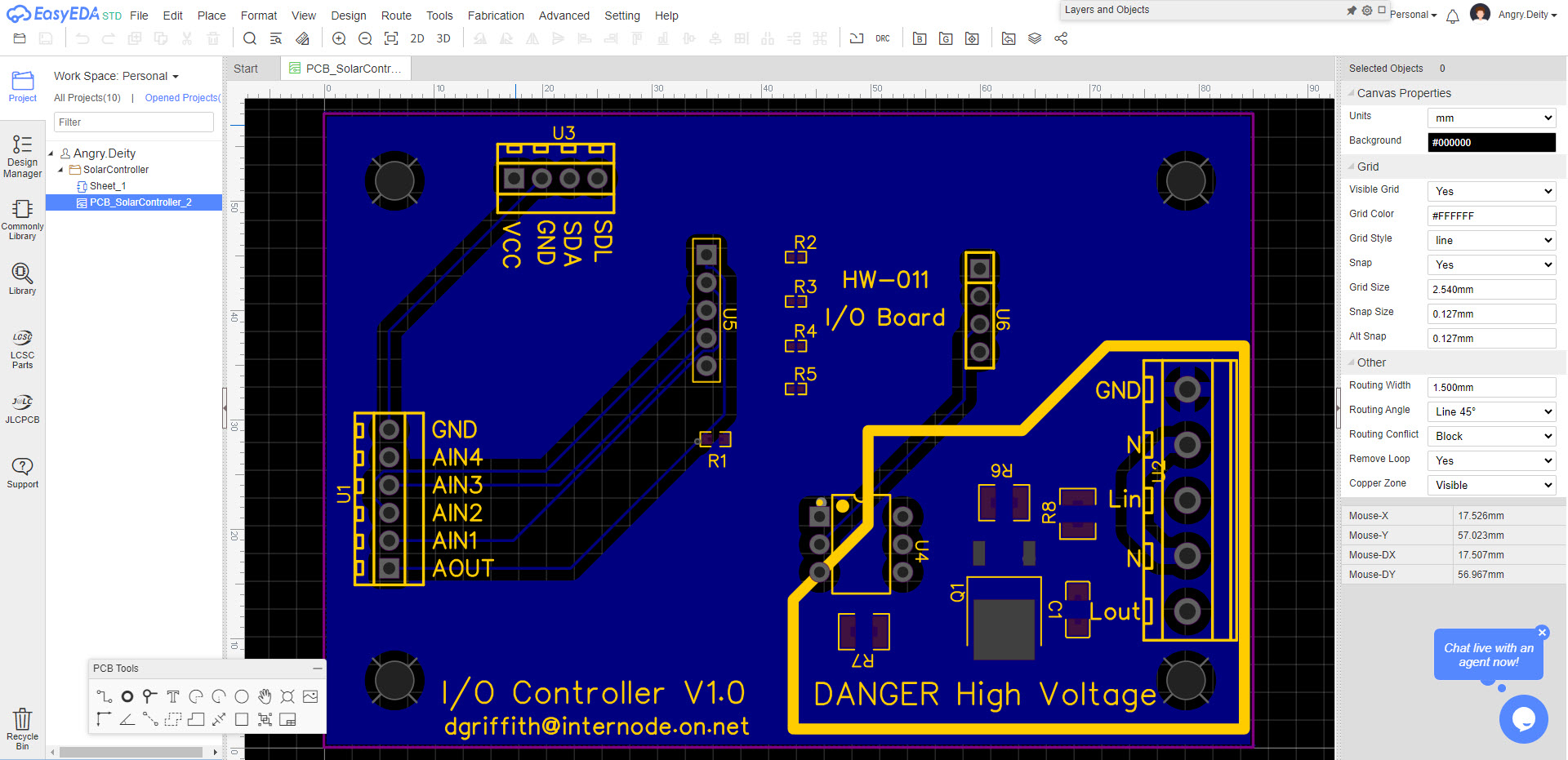
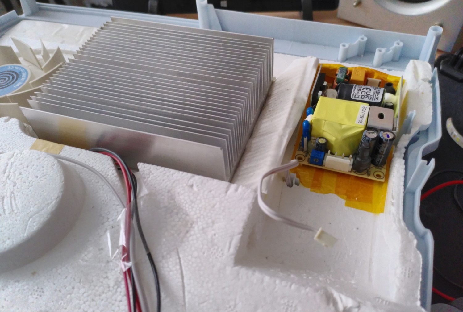
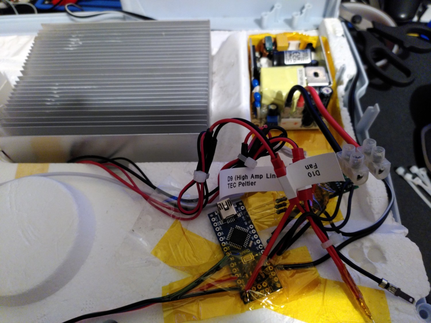
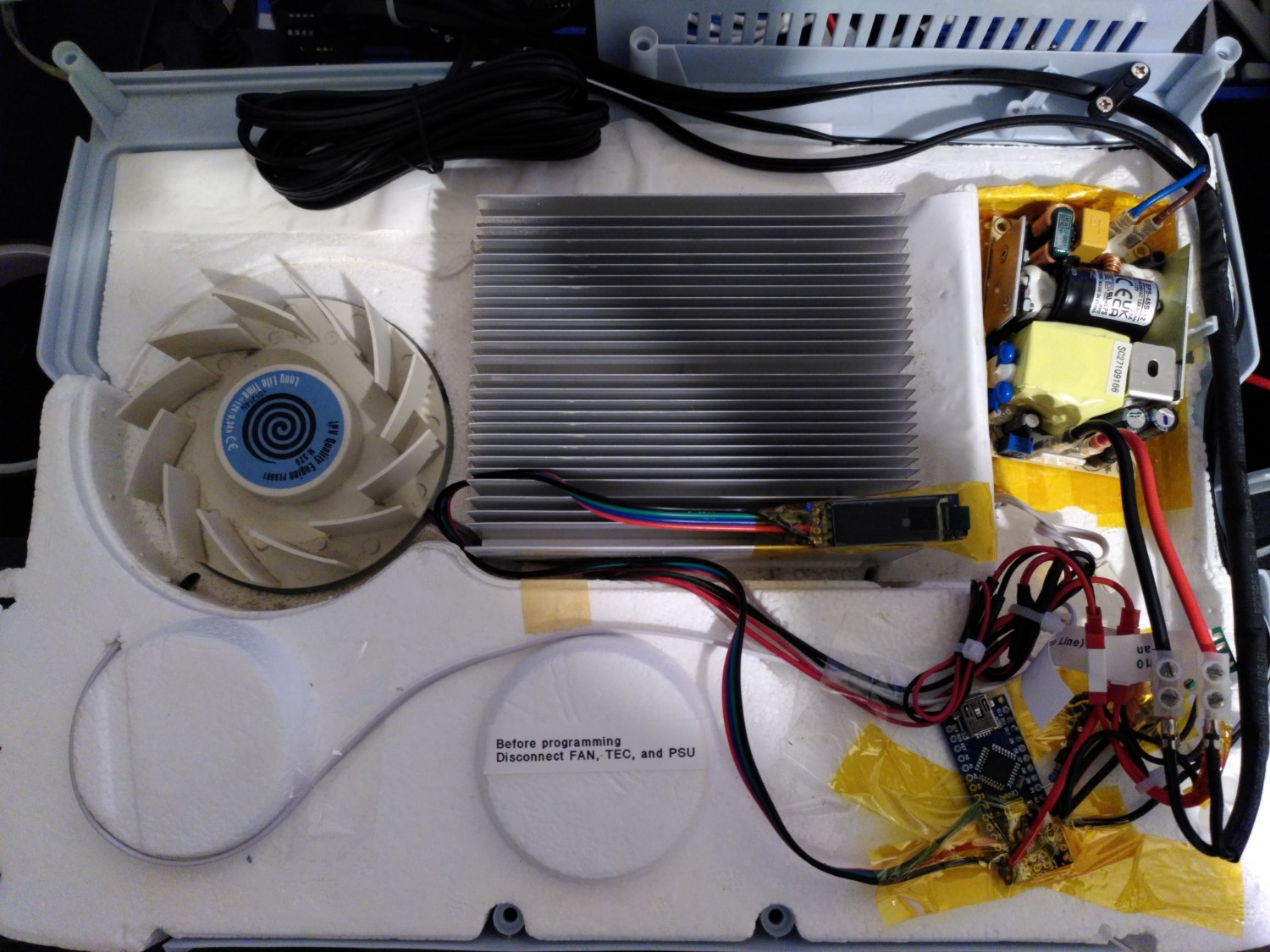
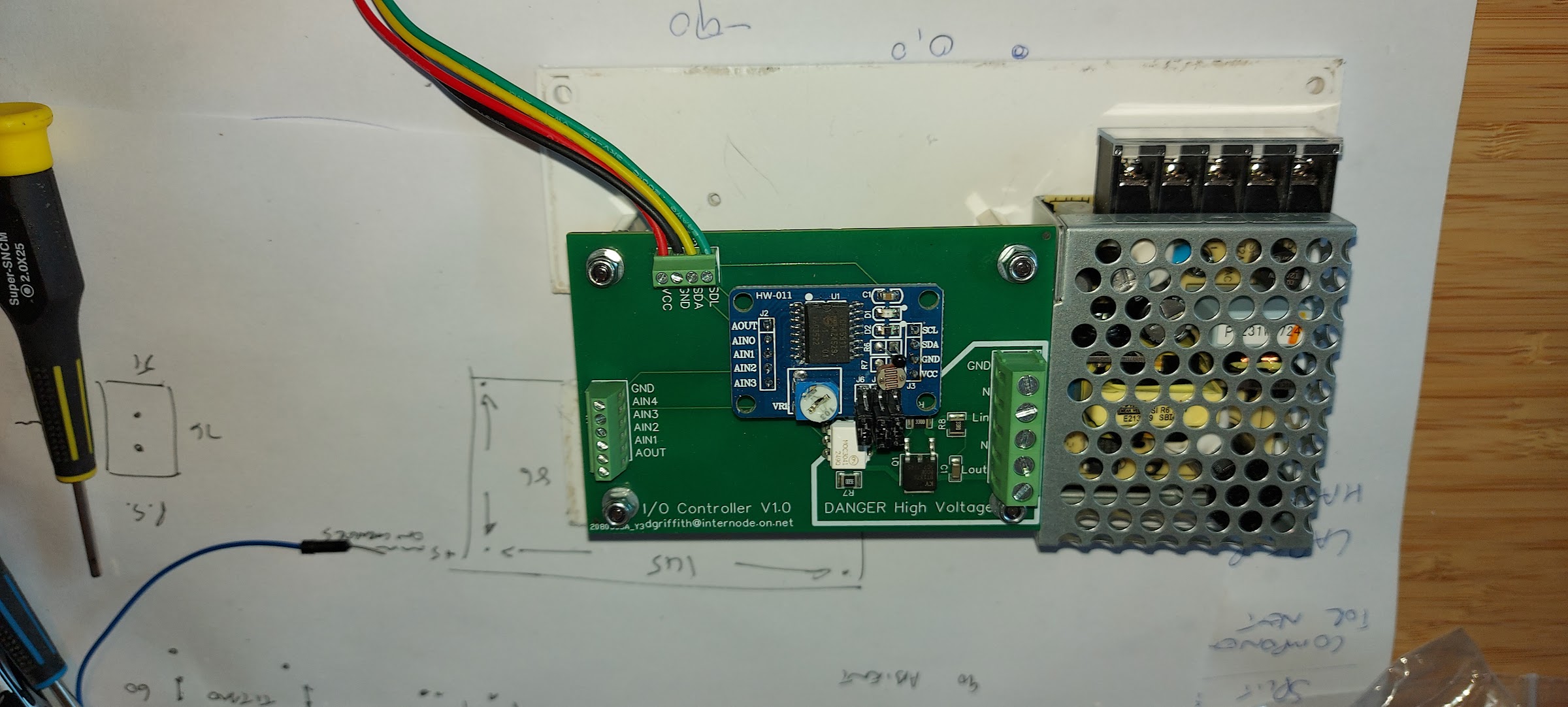
I am using an Adafruit PyPortal Titano as the controller, running circuitpython. For I/O I am using a generic ebay PCF8591 board, which provides 4 analog input and a single analog output over an I2C bus. This is inserted into a motherboard that provides pullup resistors for the analog inputs and an optocoupled zero crossing SCR driver + SCR to drive the (thankfully low power) circulating pump. Board design is my own, design is rather critical as mains supply in my country is 240V.

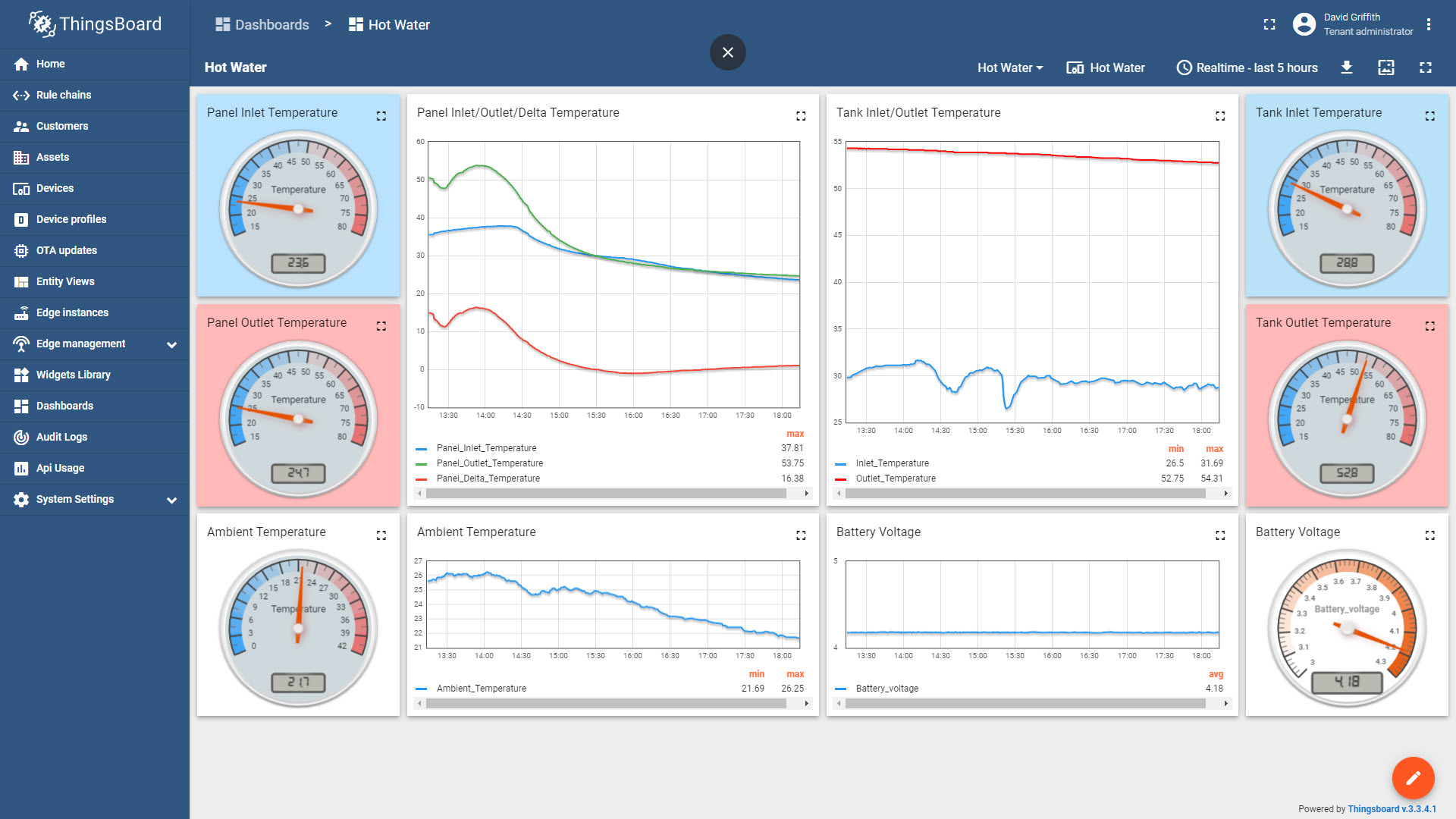
The original sensors are simple NTC thermistors, one at the bottom of the tank, and one at the top of the collector. I have also added 4 other Dallas 1-wire sensors to measure temperatures at the top of tank, ambient, tank inlet and collector pump inlet which is 1/3rd of the way up the tank. I have a duplicate of the onewire sensors already on the hot water tank using a different adafruit board and circuitpython. Their readings are currently uploaded to my own IOT server and I can plot the current system's performance, and I intend to do the same thing with this board.

The current performance is fairly dismal, a very small bump of perhaps 0.5 - 1 deg C in the normally 55 degree C tank temperature around 12pm to 1pm, and this is in Australia in hot spring weather of 28-32 degrees C.(There's some inaccuracy of the tank temperatures, the sensors aren't really bonded to the tank in any meaningful way, so tank temp is probably a little warmer than this. But I'm looking for relative temperature increases anyway)

Right now , the hardware is all together and functional, and is driving a 13W LED downlight as a test, and I can read the onewire temp sensors, read an analog voltage on the PCF8591 board (which will go to the NTC sensors), and I'm pulsing the pump output proportionally from 0-100 percent drive on a 30 second duty cycle, so that a pump drive function can simply say "run the pump at 70 percent" and you'll get 21 seconds on, 9 seconds off. Duty cycle time is adjustable, so I might lower it a bit to 15 or 10 seconds.

The next step is to try it on the circulating pump (which is quite an inductive load, even if it is only 20 watts), and start working on an algorithm that reads the sensors and maximises water temperature back to the tank. There are a few safety features that I'll put in there, such as a "fault mode" to drive the pump at a fixed rate if there is a sensor failure, and a "night cool" mode if the hot water tank is severely over temperature to circulate hot water to the collector at night to cool it. There are the usual overtemp/overpressure relief valves in the system already.

All this is going in a case with a clear hinged cover on the front so I can open it and poke the Titano's touchscreen to do some things.

Right now I am away from home from work, so my replies might be a bit sporadic, but I'll try to get back to any questions soon-ish.

A few photos for your viewing pleasure:

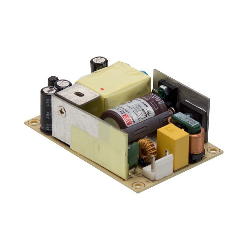
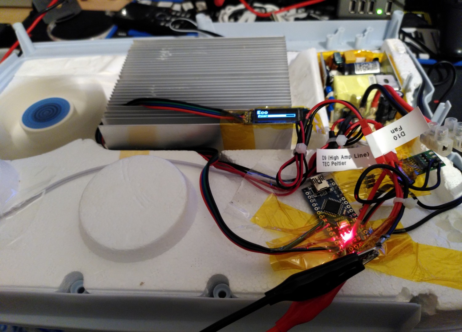
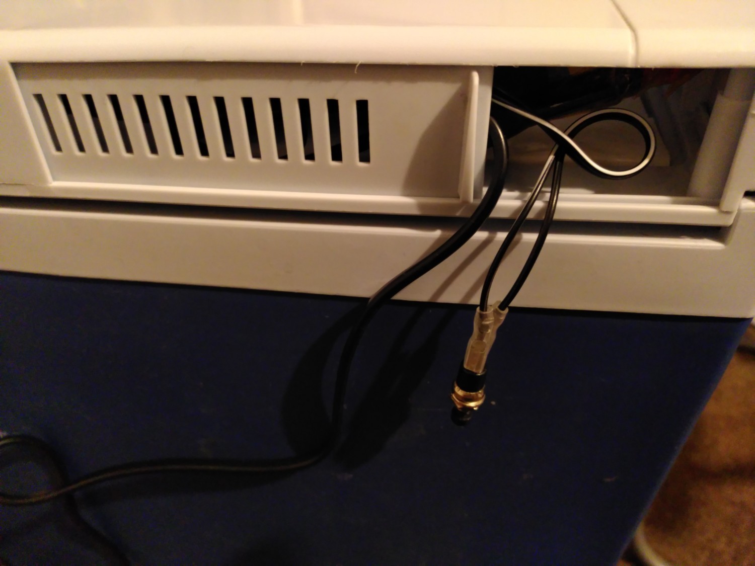
The I/O and mainboard plus a 5V power supply mounted up:

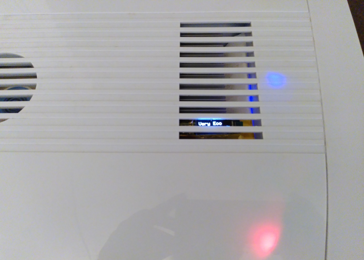
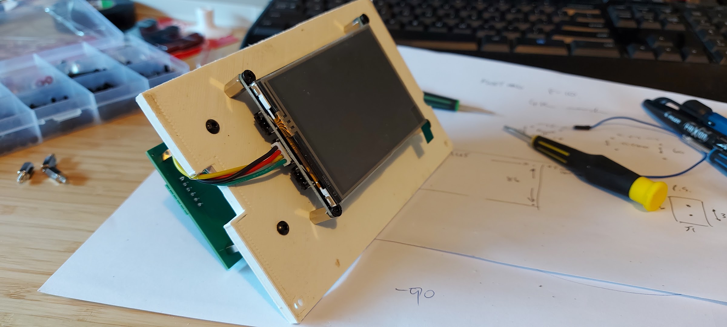
The front of the panel, showing the Pyportal:

Thingsboard display showing readings from the current system:

Mainboard PCB design and construction via EasyEDA:

10
1

Arguments to support the idea:

  • According to browse.feddit.de, this is the largest community for showcasing electronics projects, the last post is almost one month old.
  • People that signup to alien.top via the fediverserver portal will have this community as the recommended alternative to /r/electronics, but they will pretty much never see it if the community does not have any fresh content and will be more likely to lose interest.
  • Despite the usual criticism of mirroring bots, the way that the fediverser tool works is showing to actually help interaction. In the past two weeks, I'm seeing an above average increase of subscriber and (more importantly) user count on communities like !main@selfhosted.forum, !homelab@selfhosted.forum and !emacs@communick.news
11
1
A 74xx-defined Radio (acidbourbon.wordpress.com)

A shortwave radio receiver from scratch using only cheap and easily available components, i.e. standard transistors, op-amps and 74xx logic chips. No typical radio parts – no coils, no variable capacitors, no exotic diodes.

12
1
submitted 8 months ago* (last edited 8 months ago) by kjo@discuss.tchncs.de to c/electronics@discuss.tchncs.de

Not my post/video. Link to mastodon.social post which then links to YouTube video.

Poster bought an old firewall hardware:

  1. saw unpopulated footprints on the circuit board,
  2. analyzed the chips,
  3. found the serial comm to access BIOS (blocked by password),
  4. dumped the SPI flash memory,
  5. obtained supervisor password,
  6. accessed the BIOS from serial comm,
  7. enabled the video display in BIOS,
  8. soldered the HDMI port,
  9. soldered the SATA power and data ports and the associated components,
  10. connected a SATA SSD,
  11. checked that the SSD is being recognized in BIOS,
  12. made modifications to firewall circuit board to mechanically secure the SSD, and to face plate to facilitate the HDMI port,
  13. installed FreeDOS and used it as a retro gaming PC.
13
1
14
1

As solder bump pitches shrink, several issues arise. Reduced bump height and surface area for bonding make it increasingly difficult to establish reliable electrical connections, necessitating precise manufacturing processes to avoid errors. Critical co-planarity and surface roughness become paramount, as even minor irregularities can compromise successful bonding.

To overcome these issues, Cu-Cu hybrid bonding technology steps in as a game-changer. This innovative technique involves embedding metal contacts between dielectric materials and using heat treatment for solid-state diffusion of copper atoms, thereby eliminating the bridging problem associated with soldering.

The advantages of hybrid bonding over flip-chip soldering are obvious. Firstly, it enables ultra-fine pitch and small contact sizes, facilitating high I/O counts. This is critical in modern semiconductor packaging, where devices require a growing number of connections to meet performance demands. Secondly, unlike flip-chip soldering, which often relies on underfill materials, Cu-Cu hybrid bonding eliminates the need for underfill, reducing parasitic capacitance, resistance and inductance, as well as thermal resistance. Lastly, the reduced thickness of the bonded connections in Cu-Cu hybrid bonding, nearly eliminating the 10 to 30 micron thickness of solder balls in flip-chip technology, opens up new possibilities for more compact and efficient semiconductor packages.

15
1

Although you are probably not aware of them, dozens of electronic control units (ECUs) — printed circuit boards (PCBs) in metal or plastic housings — exist in your car to control and monitor the operation and safety of your vehicle’s many control systems. These units must work for the lifetime of your car, during which time they are subjected to many heating and cooling cycles. The most obvious cycle occurs when you start your car after it has cooled at night. It heats up as the car runs and then cools again when you shut it off. That’s one “ambient” temperature cycle.

Additional so called “active” thermal cycles can occur locally within specific electronic components on the PCB. For instance, a MOSFET transistor draws a lot of current and heats up the PCB near its location, causing additional thermal cycling. These complex temperature distributions can cause local thermomechanical strain because differences in temperature across the PCB result in differential expansion of the board. Because the board is constrained by its housing, this can lead to bending of the board, putting additional strain on the solder joints that connect the components to the board.

The widely used power law based approach — simulation of only few cycles and prognosis of solder joints lifetime — has many shortcomings, where no absolute lifetime prediction or the damage driven load relocation and its nonlinear evolution are captured. Youssef Maniar and Marta Kuczynska, engineers at Robert Bosch GmbH in Germany, have developed an accurate nonlinear damage model able to predict absolute lifetime of solder connections. The problem they faced, absolute lifetime prediction, involves simulation of all cycles imposed to the components, and the computational effort is therefore extensive. Then, about two years ago, they read an academic paper that described a way to “jump” over some cycles to accelerate simulation.

The mathematics behind the ability to jump over a large number of simulated thermomechanical cycles to dramatically accelerate the simulation time without sacrificing accuracy is involved, but the software essentially looks at the slope or “gradient” of certain solution variables (e.g., stress) versus time plot on the fly to determine when it can skip over the next n number of cycles. The maximum value of n must be defined by the simulation engineer before the run. The simulation engineer also inputs other parameters beforehand to impose limits on the software to optimize the run.

16
1

cross-posted from: https://discuss.tchncs.de/post/3157319

Compared with traditional monolithic devices, the design and manufacturing process for chiplets is significantly different. The scrap costs associated with manufacturing traditional monolithic semiconductor devices is basically linear, including single chip cost, packaging, and assembly costs.

Manufacturing processes for 2.5D/3D designs differ significantly in terms of the accumulation of scrap costs. Specifically, these costs increase geometrically from fabrication to assembly driven by scrap costs for multiple dies, multi-chip partial assemblies, and/or full 2.5D/3D packages.

Shifting tests, either left or right, in the test process is a strategy to achieve these goals and minimize the overall manufacturing cost of 2.5D/3D components. Shift left is the ability to increase test coverage earlier in the manufacturing process (e.g., during wafer inspection and partial packaging) to maximize KGD, while reducing future packaging costs. Additional tests can also be added to the process to identify new failure types or failure modes.

However, the benefits of shift left need to be weighed. For example, increasing test intensity early in the manufacturing process can positively impact known good devices but it can also lead to an increase in test costs that is not sufficiently offset by the optimizations, even after accounting for the resulting reduction in scrap costs.

Shift right means increasing test coverage later in the manufacturing process, expanding the ability to detect defects, and maintaining quality levels with the goal of reducing costs with higher parallelism testing.

Typically, a test item with a higher yield on wafer or mission pattern tests, or a high yield test that requires a longer scan test time is an ideal candidate for shifting right. These tests can be moved to final or system level test, or flexibly managed in between.

The goal of shifting tests to the left or right is to achieve the optimal combination of quality and yield throughout the entire manufacturing process, ultimately optimizing the overall cost of quality.

17
1

cross-posted from: https://discuss.tchncs.de/post/3011500

Many volume applications use FPGA because they need in-field reconfigurability (changing standards, changing algorithms, etc) but they want to improve their system’s competitiveness (power, size, cost). FPGAs are bulky, expensive and power hungry. Integrating eFPGA can greatly improve the economics while maintaining full reconfigurability and performance.

We’ve found with customers that a significant portion of the LUTs in their designs don’t change with reconfigurations: they are fixed buses to bring data to and from the reconfigurable core. This can be hardwired so the number of LUTs needed in the SoC is typically half of what’s in the FPGA. There is also a lot of cost of voltage regulators for an FPGA that disappear with integration.

Typically, the cost of eFPGA is 1/10th the cost of the FPGA it replaces but with the same speed and programmability. Power can also be cut to 1/10th because most of the power in an FPGA is the power-hungry PHYs that are mostly not needed when using eFPGA in the SoC.

18
1

Finally got some free time was thinking about taking up new project but it got me wondering what everyone else is working on? Please share!

19
1

I did not know about this mounting method. Probably it's a way to improve passive cooling capabilities?

20
1

cross-posted from: https://discuss.tchncs.de/post/2357238

Are you an engineer working on designing complex modern chips or System On Chips (SOCs) at the Register Transfer Level (RTL)? Have you ever been in one of the following frustrating situations?

•Your RTL designs suffered a major (and expensive) bug escape due to insufficient coverage of corner cases during simulation testing.

• You created a new RTL module and want to see its real flows in simulation, but realize this will take another few weeks of testbench development work.

• You tweaked a piece of RTL to aid synthesis or timing and need to spend weeks simulating to make sure you did not actually change its functionality.

• You are in the late stages of validating a design, and the continuing stream of new bugs makes it clear that your randomized simulations are just not providing proper coverage.

• You modified the control register specification for your design and need to spend lots of time simulating to make sure your changes to the RTL correctly implement these registers.

If so, congratulations: you have picked up the right book! Each of these situations can be addressed using formal verification (FV) to significantly increase both your overall productivity and your confidence in your results. You will achieve this by using formal mathematical tools to create orders-of-magnitude increases in efficiency and productivity, as well as introducing mathematical near-certainty into areas previously dependent on informal testing.

Design verification has always been essential to chip design. However as chip complexity increased over years, state-space and required verification effort exponentially exploded. With emerging powerful and commercially accessible tools, formal verification has become more viable and even unavoidable for reliable sign-off and catching bugs early in the process. I found this book a very helpful introduction to formal verification. It explains how formal can be utilized, different methods like formal property verification (FPV) and sequential equivalence checks (SEC) and where they are useful, limitations, complexity problems and how to mitigate the issues that come with formal. It explains how formal and functional can complement each other for combined sigh-off. It explains theoretical concepts with clear examples and diagrams. It explains formal algorithms as well for anyone interested, but focus is more about how to utilize formal in your projects. And if you are a total beginner, do not worry, there is section which explains essentials of Systemverilog Assertions (SVA), which you can completely skip if you know about it already.

21
1
22
1
submitted 10 months ago by Spzi@lemm.ee to c/electronics@discuss.tchncs.de

Topics covered in this informative video: potentiometer, electrical engineering, basic electronics, what is a resistor, resistors in series, variable resistor, power electronics, current limiting, Carbon film, carbon composite, Metal film, Potentiometer, Thermistor, RTD, LDR, Light dependant resistor, SMD, rheostat and much much more.

The video often (not always) describes resistors as coiled wires. Don't they induce magnetic fields and currents in other components? This article answered these questions for me: https://eepower.com/resistor-guide/resistor-fundamentals/resistor-inductance/#

TL;DR: Yes, but the effect is often negligible or the application does not care. When it matters, we can minimize the effect with appropriate designs (i.e. without coiled resistors).

23
1

Using Intel CPU JTAG to dump the secret bootrom in Microsoft's original Xbox. Disclaimer: not my blog.

24
1
25
1
submitted 11 months ago* (last edited 11 months ago) by nothacking@discuss.tchncs.de to c/electronics@discuss.tchncs.de

Other side:

Schematic:

view more: next ›

Electronics

1875 readers
1 users here now

Projects, pictures, industry discussions and news about electronic engineering & component-level electronic circuits.

Rules

1: Be nice.

2: Be on-topic (eg: Electronic, not electrical).

3: No commercial stuff, buying, selling or valuations.

4: No circuit design or repair, tools or component questions.

5: No excessively promoting your own sites, social media, videos etc.


Ask questions in https://discuss.tchncs.de/c/askelectronics


founded 1 year ago
MODERATORS